Architecture
This chapter describes the architecture of the eMac computer. It includes information about the major components on the main logic board: the microprocessor, the other main ICs, and the buses that connect them to each other and to the I/O interfaces.
In this section:
Block Diagram and Buses
Microprocessor and Cache
Uni-N Bridge and Memory Controller
KeyLargo I/O Controller
Block Diagram and Buses
This section is an overview of the major ICs and buses on the computer’s main logic board.
Block Diagram
Figure 2-1 is a simplified block diagram of the main logic board. The diagram shows the main ICs and the buses that connect them together.
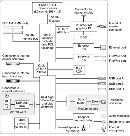
Main ICs and Buses
The architecture of the eMac is designed around the PowerPC G4 microprocessor and and two custom ICs: the Uni-N memorycontroller and bus bridge, and the KeyLargo I/O controller.
The eMac computer has four major buses.
processor bus: 100 MHz, 64-bit bus connecting the processor module to the Uni-N IC
memory bus: 100 MHz, 64-bit bus connecting the main memory to the Uni-N IC
AGP bus: 66 MHz, 32-bit bus connecting the AGP card to the Uni-N IC
PCI bus: 33 MHz, 32-bit bus connecting the boot ROM to the KeyLargo I/O controller.
The remainder of this chapter describes the architecture in three sections centered around the processor module, the Uni-N memory controller and bridge IC, and the KeyLargo I/O controller IC.
Microprocessor and Cache
The microprocessor is a PowerPC G4 with a built-in level 2 (L2) cache.
PowerPC G4 Microprocessor
The PowerPC G4 microprocessor used in the eMac computer has many powerful features, including a pipelined system bus called MaxBus.
The PowerPC G4 has the following features:
32-bit PowerPC implementation
superscalar PowerPC core
Velocity Engine (AltiVec technology): 128-bit wide vector execution unit
high bandwidth MaxBus
dual 32 KB instruction and data caches (level 1)
built-in 256 KB backside L2 cache
To find more information, see the reference at “PowerPC G4 Microprocessor.”
Level 2 Cache
The data storage for the L2 cache consists of 256 KB of fast static RAM that is built into the microprocessor chip along with the cache controller. The built-in L2 cache runs at the same clock speed as the microprocessor.
Uni-N Bridge and Memory Controller
The Uni-N custom IC is at the heart of the computer. It provides the bridging functionality between the processor, the memory system, the PCI-based I/O system, the AGP slot, and the FireWire and Ethernet interfaces.
Processor Bus
The processor bus is a 100 MHz, 64-bit bus connecting the processor module to the Uni-N IC. In addition to the increased bus clock speed, the bus uses MaxBus protocols, supported by the Uni-N IC, for improved performance.
The MaxBus protocol includes enhancements that improve bus efficiency and throughput over the 60x bus. The enhancements include
out of order completion
address bus streaming
intervention
Out of order completion allows the memory controller to optimize the data bus efficiency by transferring whichever data is ready, rather than having to pass data across the bus in the order the transactions were posted on the bus. This means that a fast DRAM read can pass a slow PCI read, potentially enabling the processor to do more before it has to wait on the PCI data.
Address bus streaming allows a single master on the bus to issue multiple address transactions back-to-back. This means that a single master can post addresses at the rate of one every two clocks, rather thanone every three clocks, as it is in the 60x bus protocol.
Intervention is a cache-coherency optimization that improves performance for dual processor systems. If one processor modifies some data, that data first gets stored only in that processor’s cache. If the other processor then wants that data, it needs to get the new modified values. In previous systems, the first processor must write the modified data to memory and then the second processor can read the correct values from memory. With intervention, the first processor sends the data directly to the second processor, reducing latency by a factor of ten or more.
Main Memory Bus
The main memory bus is a 100 MHz, 64-bit bus connecting the main memory to the Uni-N IC. The memory interface is synchronized to the 60x bus interface at 100 MHz.
Main memory is provided by one or two PC-133 DIMMs (dual inline memory modules). For more information about memory DIMMs, see “RAM Expansion.”
Accelerated Graphics Port Bus
The accelerated graphics port (AGP) bus is a 66 MHz, 32-bit bus connecting the AGP IC to the Uni-N IC. The AGP bus provides faster access to main memory than previous designs using the PCI bus.
The AGP bus is a superset of the PCI bus, with the addition of separate address lines so it does not multiplex address and data when running in AGP mode. Having a separate address bus allows the AGP bus to pipeline addresses, thereby improving performance.
To further improve the performance of the AGP bus, the Uni-N IC supports a graphics address remapping table (GART). Because the virtual memory system organizes main memory as randomly distributed 4 KB pages, DMA transactions for more than 4 KB of data must perform scatter-gather operations. To avoid this necessity for AGP transactions, the GART is used by the AGP bridge in the Uni-N to translate a linear address space for AGP transactions into physical addresses in main memory.
Video Display Subsystem
The display subsystem consists of a graphics controller IC and 32 MB of DDR on the main logic board. The graphics controller IC is an NVidia GeForce2 MX. It contains 2D and 3D acceleration engines, front-end and back-end scalers, a CRT controller, and an AGP bus interface with bus master capability.
The interface between the graphics IC and the rest of the system is an AGP (accelerated graphics port) bus on the Uni-N IC. To give the graphics IC fast access to system memory, the AGP bus has separate address and data lines and supports deeply pipelined read and write operations. The AGP bus has 32 data lines and a clock speed of 66 MHz.
The graphics IC uses a graphics address remapping table (GART) to translate AGP logical addresses into physical addresses. The graphics driver software can allocate memory in both the dedicated SDRAM and the main memory.
For information about the display and supported resolutions, see “Video Display.”
PCI Bus
The PCI bus connects the Uni-N IC to the boot ROM and the KeyLargo I/O controller. The PCI bus is a 33 MHz, 64-bit bus.
The Uni-N IC used in the eMac computer supports a PCI feature called write combining. This feature allows sequential write transactions involving the Memory Write or Memory Write and Invalidate commands to be combined into a single PCI transaction. The memory write transactions being combined must be to sequential, ascending, and non-overlapping PCI addresses. Placing an eieio or sync command between the write commands prevents any write combining.
Boot ROM
The boot ROM consists of 1 MB of on-board flash EPROM. The boot ROM includes the hardware-specific code and tables needed to start up the computer, to load an operating system, and to provide common hardware access services.
Ethernet Controller
The Uni-N IC includes an Ethernet media access controller (MAC). As a separate I/O channel on the Uni-N IC, it can operate at its full capacity without degrading the performance of other peripheral devices. The MAC also provides DMA support for the Ethernet interface.
The MAC implements the link layer. It is connected to a PHY interface IC that provides 10Base-T or 100Base-T operation over a standard twisted-pair interface. The operating speed of the link is automatically negotiated by the PHY and the bridge or router to which the Ethernet port is connected. For information about the port, see “Ethernet Port.”
FireWire Controller
The Uni-N IC includes an IEEE 1394 FireWire controller that implements the FireWire link layer. The controller supports a maximum data rate of 400 Mbits (50 MBytes) per second.
The controller IC implements the FireWire link layer. A physical layer IC, called a PHY, implements the electrical signalling protocol of the FireWire interface. The PHY supports two FireWire ports by way of external connectors in the I/O bay.
The PHY is powered as long as the computer is connected to AC power. While the PHY is operating, it acts as a repeater from one port to another so that the FireWire bus remains connected. For more information, see “FireWire Ports.”
KeyLargo I/O Controller
The KeyLargo custom IC is the third major component of the architecture. It provides all the I/O functions except Ethernet and FireWire. The KeyLargo IC provides two USB root hubs, an Ultra DMA/66 interface, and support for the communication slot and the sound IC.
DMA Support
The KeyLargo IC provides DB-DMA (descriptor-based direct memory access) support for the following I/O channels:
Ultra DMA/66 interface
communication slot interface
IIS channel to the sound subsystem
The DB DMA system provides a scatter-gather process based on memory-resident data structures that describe the data transfers. The DMA engine is enhanced to allow bursting of data files for improved performance.
Interrupt Support
The interrupt controller for the eMac computer is an MPIC cell in the KeyLargo IC. In addition to accepting all the KeyLargo internal interrupt sources, the MPIC controller accepts external interrupts from dedicated interrupt pins and serial interrupts from the Uni-N serial interrupt stream. The signals from the Uni-N IC are synchronized to the operation of the MPIC circuitry, so there is no additional interrupt latency on the Uni-N interrupts.
USB Interface
The KeyLargo IC implements two independent USB root hubs. USB port A is connected to one controller and the other two USB ports are connected to the other. The use of two independent hubs allows both USB ports to support high data rate devices at the same time with no degradation of their performance. Thus, if a user connects a high-speed (12 Mbps) device to USB port A and another high-speed device to the port B, both devices can operate at their full data rates.
Internally, the second port of one controller is routed to the modem slot for an internal USB modem. The second port of the other controller is connected to the third external USB port.
The external USB connectors support USB devices with data transfer rates of 1.5 Mbps or 12 Mbps. For more information about the connectors, see “USB Ports.”
USB devices connected to the eMac are required to support USB-suspend mode as defined in the USB specification. Information about the operation of USB-suspend mode on Macintosh computers is included in the Mac OS USB DDK API Reference. To obtain that document, please see the references at “USB Interface.”
The USB ports on the eMac computer comply with the Universal Serial Bus Specification 1.1 Final Draft Revision. The USB controllers comply with the Open Host Controller Interface (OHCI) specification.
Ultra DMA Interface
In the eMac computer, the KeyLargo IC provides an Ultra DMA IDE (integrated drive electronics) channel that is connected to the internal hard disk drive. The Ultra DMA IDE interface, also called Ultra-DMA/66 and ATA-5, is an improved version of the EIDE interface.
The KeyLargo IC provides DB-DMA (descriptor-based direct memory access) support for the Ultra DMA interface.
The cable is wired to select the internal hard disk drive as device 0 (master) in an ATA Device 0/1 configuration.
Enhanced IDE Interface
In the eMac computer, the KeyLargo IC provides an enhanced IDE (EIDE) interface that supports the internal Combo (DVD-ROM and CD-RW) disk drive.
The EIDE interface uses multiword DMA. The Combo drive is connected as device 0 (master) in an ATA Device 0/1 configuration.
For information about the Combo drive, see “Combo Drive DVD-ROM/CD-RW.”
Modem Slot Support
The KeyLargo IC has a traditional Macintosh serial port that is connected to the modem slot. The KeyLargo IC also provides digital audio to the slot in the form of an IIS port that shares pins with the serial port.
The KeyLargo IC provides DB-DMA (descriptor-based direct memory access) support for the modem slot interface.
The internal hardware modem is a separate module that contains the datapump IC and the interface to the telephone line (DAA). For more information about the modem, see “Internal Modem.”
Wireless LAN Module
The interface between the wireless LAN module and the KeyLargo IC is similar to a PC Card interface.
The wireless LAN module contains a media access controller (MAC), a digital signal processor (DSP), and a radio-frequency (RF) section. The module has a connector for the cable to the antennas, which are built into the computer’s enclosure.
The wireless LAN module is based on the IEEE 802.11 standard. The wireless LAN module transmits and receives data at up to 11 Mbps and is compatible with older systems that operate at 1 or 2 Mbps. For information about its operation, see “AirPort Card.”
Sound Circuitry
The sound circuitry is designed around a set of ICs called Snapper and is connected to the KeyLargo IC by standard IIC and IIS buses. The IIC bus provides configuration access to the Snapper ICs and the IIS bus is used for data transfers. The KeyLargo IC provides DB-DMA (descriptor-based direct memory access) support for the IIS port.
The Snapper circuitry performs digital audio processing and codec functions. The audio processing functions include output equalization and volume control. The codec functions include A-to-D and D-to-A conversion.
Stereo signals from the sound input jack drive Snapper’s A-to-D converter. Audio data from the KeyLargo IC drives Snapper’s D-to-A converter. Analog output from the D-to-A converter is routed to the headphone jack and the audio power amplifier.
The power amplifier drives the internal speaker. When headphones are connected to the headphone jack, the internal speaker is muted.
For a description of the features of the sound system, see “Sound System.”
Power Controller
The power management controller in the eMac is a custom IC called the PMU99. It supports several power-saving modes of operation, including idle, doze, and sleep.
© 2002 Apple Computer, Inc. All Rights Reserved. (Last updated: 2002-10-01)